The memory subsystem was the first component of my 4-bit processor that actually got built. Initially, my goal was less ambitious; I picked up some surplus 4×256 bit static RAM chips at a local electronics store, and I just wanted to see if I can build a simple circuit to store, and retrieve, data from these chips.
This didn't turn out to be a useless exercise, however. The DIP switches I used to exercise the memory chip are still used to load programs and data into my processor's memory. A planned modification to this circuit will also reuse the DIP switches and one of the LED displays to load, and display, I/O data which will allow my processor to interface with the outside world.
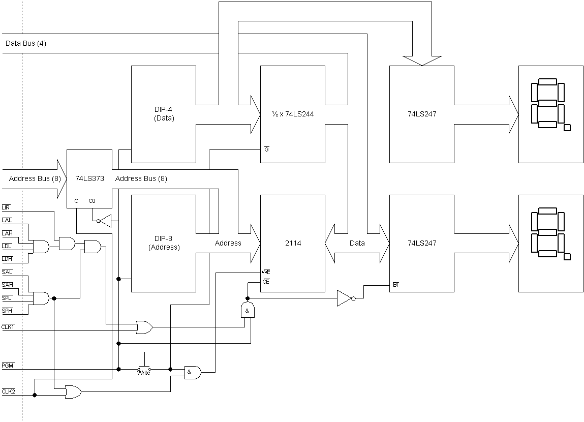
The memory subsystem interfaces with other components via the Data Bus and the Address Bus. The Data Bus is bidirectional; data can be both read and written. The Address Bus is unidirectional; addresses are generated by other processor components and are used by the memory subsystem to select the appropriate memory location for reading or writing.
In addition to the data and address buses, the memory subsystem also receives decoded instruction microcodes. These instruction microcodes control the operation of the subsystem. Specifically, nine instruction microcodes are recognized by this subsystem, decoded into one state and one trigger condition.
Microcodes LIR, LAL, LAH, LDL and LDH cause the subsystem to enter the MRD (Memory ReaD) state. In this state, the contents of memory appear on the Data Bus as output. The address from the Address Bus is used to select the desired memory location.
Microcodes SAL, SAH, SPL and SPH cause the subsystem to execute the MWR (Memory WRite) trigger. On the negative edge of CLK2, the memory subsystem fetches whatever data is on the Data Bus and stores it at the current address that is present on the Address Bus.
Finally, an additional signal (denoted PGM in the diagram below) indicates whether the processor is in its normal, operational state, or in the manual programming state. In the manual programming state, the memory contents can be read, and set, using the DIP switches that are part of the memory subsystem.