Perhaps the most interesting question with any processor is this: how do instruction codes (i.e., code words in memory) get turned into electrical signals that in turn trigger various events in the processor, altering its internal state?
There are many solutions to this problem, one of which is the use of microcode. While machine instructions are designed with the user in mind (well, inasmuch as machine language can be code user-friendly, that is!), microcode instructions represent internal state changes of the machine itself.
In the case of my 4-bit contraption, each machine code instruction is translated into several microcode instructions. Each microcode "instruction" is really just an electrical signal that, along with the clock signals activates various components of the processor. One of the tricks is the use of a two-phase clock, whose signals look like this:
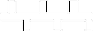
As you can see, the first clock signal transitions from a high to a low state before the second clock signal. When the first clock signal is in a low state, subsystems in the processor respond by presenting information on their outputs, but without altering their internal states. When the second clock signal transitions from a high-state to a low state, subsystems respond by latching whatever data is present on their inputs and alter their internal state.
Designing the microcode set was only possible after I have developed the functional block diagram for the entire processor, and had more than a clue about the way its main components will work. The finalized microcode instruction set consists of 22 microcode instructions:
| Opcode | Instruction | Mnemonic | CLK1 (states) | CLK2 (triggers) |
| 00 | Halt | HLT | HLT | - |
| 01 | Load Instruction Register | LIR | APC+MRD+PCI+INC | LIR+LPC |
| 02 | Load AC low nybble from [DA]* | LAL | ADA+SDA+MRD+INC | LDL+LDA |
| 03 | Load AC high nybble from [DA] | LAH | ADA+MRD | LDH |
| 04 | Load DA low nybble from PC | LDL | APC+MRD+PCI+INC | LDL+LPC |
| 05 | Load DA high nybble from PC | LDH | APC+MRD+PCI+INC | LDH+LPC |
| 06 | Store AC low nybble to [DA]* | SAL | ADA+SAL+SDA+INC | MWR+LDA |
| 07 | Store AC high nybble to [DA] | SAH | ADA+SAH | MWR |
| 08 | Store PC low nybble to [DA] | SPL | ADA+SPL+SDA+INC | MWR+LDA |
| 09 | Store PC high nybble to [DA] | SPH | ADA+SPH | MWR |
| 0A | Load PC from DA | LPC | SDA+TWO | LPC |
| 0B | Load PC on No Carry | PCC | SDA+TWO | ~C->LPC |
| 0C | Load PC on No Data | PCD | SDA+TWO | ~D->LPC+CLD |
| 0D | Load PC on No Zero | PCZ | SDA+TWO | ~Z->LPC |
| 0E | Store AC&DA to AC | AND | SAC+SDA+AND | LAC+STF |
| 0F | Store AC|DA to AC | OR | SAC+SDA+OR | LAC+STF |
| 10 | Store AC+DA to AC | ADD | SAC+SDA+ADD | LAC+STF |
| 11 | Store AC-DA from AC | SUB | SAC+SDA+SUB | LAC+STF |
| 12 | Compute AC-DA | CMP | SAC+SDA+SUB | STF |
| 13 | Rotate Left | ROL | SAC+ROL | LAC+STF |
| 14 | Rotate Right | ROR | SAC+ROR | LAC+STF |
| 15 | Clear Flags | CLF | - | CLF |
*Use of square brackets implies indirection (e.g., store at [DA] means store in memory at the address in DA.)
The two rightmost columns tell us what happens in the various subsystems during the two clock phases. I called CLK1 events states (because they alter the output state of subsystems) and CLK2 events triggers (because they trigger an internal change upon the high-to-low transition of the clock signal.)
These states and triggers are essentially internally decoded electrical signals inside each subcomponent. They are described in detail along with the appropriate subcomponent's detailed description.
So now we can translate the 16 machine language instructions into microcode instructions:
| Opcode | Microcode |
| HLT | HLT,LIR |
| LDA | LDL,LDH,LAL,LAH,LIR |
| STA | LDL,LDH,SAL,SAH,LIR |
| JMP | LDL,LDH,LPC,LIR |
| SPC | LDL,LDH,SPL,SPH,LIR |
| AND | LDL,LDH,AND,LIR |
| OR | LDL,LDH,OR,LIR |
| ADD | LDL,LDH,ADD,LIR |
| SUB | LDL,LDH,SUB,LIR |
| CMP | LDL,LDH,CMP,LIR |
| JNZ | LDL,LDH,PCZ,LIR |
| JND | LDL,LDH,PCD,LIR |
| JNC | LDL,LDH,PCC,LIR |
| ROL | ROL,LIR |
| ROR | ROR,LIR |
| CLF | CLF,LIR |
So what does this all mean? Let's take, for instance, the LDA instruction. In plain English, this instruction accomplishes the following:
- Fetches the next two machine words into the internal Data Address Register, while incrementing the Program Counter
- Loads data at the address stored in the Data Address Register into the Accumulator
It is translated into five microcode instructions, which in turn cause the following to happen:
| Microcode | State/ Trigger |
Description |
| LDL | APC | PC places its current value on the address bus |
| PCI | PC places its current value on ALU's input | |
| MRD | Memory places its output at current address on data bus | |
| INC | ALU places input + 1 on its output | |
| LDL | DA fetches the contents of the data bus to its lower half | |
| LPC | PC fetches the ALU output | |
| LDH | APC | PC places its current value on the address bus |
| PCI | PC places its current value on ALU's input | |
| MRD | Memory places its output at current address on data bus | |
| INC | ALU places input + 1 on its output | |
| LDH | DA fetches the contents of the data bus to its upper half | |
| LPC | PC fetches the ALU output | |
| LAL | ADA | DA places its current value on the address bus |
| SDA | DA places its current value on ALU's input | |
| MRD | Memory places its output at current address on data bus | |
| INC | ALU places address bus + 1 on its output | |
| LDL | AC fetches the contents of the data bus to its lower half | |
| LDA | DA fetches the ALU output | |
| LAH | ADA | DA places its current value on the address bus |
| MRD | Memory places its output at current address on data bus | |
| LDH | AC fetches the contents of the data bus to its upper half | |
| LIR | APC | PC places its current value on the address bus |
| MRD | Memory places its output at current address on data bus | |
| INC | ALU places address bus + 1 on its output | |
| LIR | SEQ fetches instruction word from data bus and resets microcode counter | |
| LPC | PC fetches the ALU output |
The states and triggers are decoded by logic circuits inside the individual subsystems. As you can see, there's a lot of repetitiveness here, but that's precisely the point: the goal here is to reduce relatively complex instructions into simple, repetitive operations that can then be implemented in hardware.
The table below cross-references all 22 microcode instructions with states and triggers in each subsystem.
|
Microcode Instructions |
||||||||||||||||||||||
|
State/ |
HLT | LIR | LAL | LAH | LDL | LDH | SAL | SAH | SPL | SPH | LPC | PCC | PCD | PCZ | AND | OR | ADD | SUB | CMP | ROL | ROR | CLF |
|
Accumulator |
||||||||||||||||||||||
| LAC/LAC | X | X | X | X | X | X | ||||||||||||||||
| LAH/LAH | X | |||||||||||||||||||||
| LAL/LAL | X | |||||||||||||||||||||
| SAC/ | X | X | X | X | X | X | X | |||||||||||||||
| SAH/ | X | |||||||||||||||||||||
| SAL/ | X | |||||||||||||||||||||
|
Program Counter |
||||||||||||||||||||||
| APC/ | X | X | X | |||||||||||||||||||
| /LPC | X | X | X | X | C | D | Z | |||||||||||||||
| PCI/ | X | X | X | |||||||||||||||||||
| SPH/ | X | |||||||||||||||||||||
| SPL/ | X | |||||||||||||||||||||
|
Data Address |
||||||||||||||||||||||
| ADA/ | X | X | X | X | X | X | ||||||||||||||||
| DAI/ | ||||||||||||||||||||||
| LDA/LDA | X | X | X | |||||||||||||||||||
| LDH/LDH | X | |||||||||||||||||||||
| LDL/LDL | X | |||||||||||||||||||||
| SDA/ | X | X | X | X | X | X | X | X | X | X | X | X | ||||||||||
|
ALU |
||||||||||||||||||||||
| ADD/ | X | |||||||||||||||||||||
| AND/ | X | |||||||||||||||||||||
| /CLD | X | |||||||||||||||||||||
| /CLF | X | |||||||||||||||||||||
| CMP/ | ||||||||||||||||||||||
| OR / | X | |||||||||||||||||||||
| ROL/ | X | |||||||||||||||||||||
| ROR/ | X | |||||||||||||||||||||
| /STF | X | X | X | X | X | X | X | |||||||||||||||
| SUB/ | X | X | ||||||||||||||||||||
| TWO/ | X | X | X | X | ||||||||||||||||||
| INC/ | X | X | X | X | X | X | X | |||||||||||||||
| Sequencer | ||||||||||||||||||||||
| HLT/ | X | |||||||||||||||||||||
| /LIR | X | |||||||||||||||||||||
| Memory | ||||||||||||||||||||||
| MRD/ | X | X | X | X | X | |||||||||||||||||
| /MWR | X | X | X | X | ||||||||||||||||||
An interesting side note about this design is that despite its simplicity, it actually does some parallel execution, a feature of modern, high-speed processors. Take a look at the LDL microcode instruction, for instance. Loading the DA register from memory doesn't involve using the ALU, so it is possible to exercise the ALU in parallel, using it to increment the program counter.
But the microcode sequencer isn't responsible for executing microcode instructions (except, of course, for microcode instructions that affect the sequencer itself.) It is merely responsible for generating microcode instructions in the proper sequence from machine instructions. Microcode instructions are completely decoded; i.e., there are 22 individual control lines, one for each instruction.
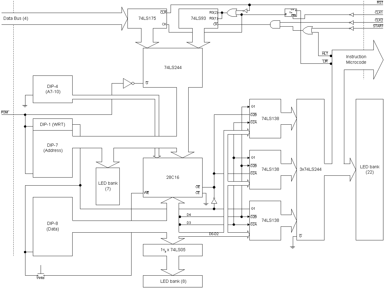
Microcode is stored in a Flash ROM; an oversized Flash ROM in this case, but it so happens that that's what I had in my toolbox! It is a 28C16 Flash ROM from Microchip.
The sequencer circuit (shown below) also contains a series of DIP switches that are used to program the Flash ROM. These DIP switches are not strictly necessary; you can also use an external programmer. In my case, for one thing I didn't have an appropriate programmer unit handy when I was building this circuit, and I also found it convenient to program the chip in-circuit. Hence, the switches.
So, how does this thing work? Four-bit instruction codes are fetched from the data bus by a 74LS175 quad flip-flop. The instruction word is represents the upper 4 bits of the microcode address. The lower 4 bits are generated by a 74LS93 counter, leaving room for a maximum of 16 microcode words per instruction. The counter is controlled by the clock signals, the HLT and the LIR microcode instructions, and the START line (which is pulled low by a manually operated button).
The complete 8-bit microcode address is fed to the 28C16 via a 74LS244 octal buffer. The output of the 28C16 is then decoded into 22 individual lines using three 74LS138 3-to-8 demultiplexers. LEDs are also used to show the current state of the 22 control lines; I found this very helpful while testing/debugging the circuit.
Lastly, here's the actual microcode table, used to program the 28C16:
| Opcode | Address | Microcode words (binary) | Hex | Mnemonic |
| 0 HLT | (00) 00000000 | 00000 00001 00000 00000 00000 | 00 01 | HLT,LIR |
| 1 LDA | (10) 00010000 | 00100 00101 00010 00011 00001 | 04 05 02 03 01 | LDL,LDH,LAL,LAH,LIR |
| 2 STA | (20) 00100000 | 00100 00101 00110 00111 00001 | 04 05 06 07 01 | LDL,LDH,SAL,SAH,LIR |
| 3 JMP | (30) 00110000 | 00100 00101 01010 00001 00000 | 04 05 0A 01 | LDL,LDH,LPC,LIR |
| 4 SPC | (40) 01000000 | 00100 00101 01000 01001 00001 | 04 05 08 09 01 | LDL,LDH,SPL,SPH,LIR |
| 5 AND | (50) 01010000 | 00100 00101 01110 00001 00000 | 04 05 0E 01 | LDL,LDH,AND,LIR |
| 6 OR | (60) 01100000 | 00100 00101 01111 00001 00000 | 04 05 0F 01 | LDL,LDH,OR ,LIR |
| 7 ADD | (70) 01110000 | 00100 00101 10000 00001 00000 | 04 05 10 01 | LDL,LDH,ADD,LIR |
| 8 SUB | (80) 10000000 | 00100 00101 10000 00001 00000 | 04 05 11 01 | LDL,LDH,SUB,LIR |
| 9 JNZ | (90) 10010000 | 00100 00101 01101 00001 00000 | 04 05 0D 01 | LDL,LDH,PCZ,LIR |
| A CMP | (A0) 10100000 | 00100 00101 10010 00001 00000 | 04 05 12 01 | LDL,LDH,CMD,LIR |
| B JND | (B0) 10110000 | 00100 00101 01100 00001 00000 | 04 05 0C 01 | LDL,LDH,PCD,LIR |
| C JNC | (C0) 11000000 | 00100 00101 01011 00001 00000 | 04 05 0B 01 | LDL,LDH,PCC,LIR |
| D ROL | (D0) 11010000 | 10011 00001 00000 00000 00000 | 13 01 | ROL,LIR |
| E ROR | (E0) 11100000 | 10100 00001 00000 00000 00000 | 14 01 | ROR,LIR |
| F CLF | (F0) 11110000 | 10101 00001 00000 00000 00000 | 15 01 | CLF,LIR |
Only the bits shown here need to be programmed. Other bits are ignored. These include the top 3 bits of each microcode word, as well as unused words, such as the words at address 00010005 to 0001000F (the LDA instruction only uses five microcode words, at address 00010000-00010004.) This microcode table could also have been implemented as a diode ROM instead of wasting so much useful space in my 28C16; an address decode logic could have been used in conjunction with approx. 90 diodes.